Emu10k1 Patent Info
WO9901813A1: AUDIO
EFFECTS PROCESSOR WITH MULTIPLE ASYNCHRONOUS AUDIO
STREAMS
US5928342: Audio effects processor integrated on a single
chip with a multiport memory onto which multiple
asynchronous digital sound samples can be concurrently
loaded
ABSTRACT:
A sound processor integrated on a single chip with
multiple digital sound sample stream inputs. Each input
is independently connected to separate ports of a
multi-port memory. The architecture allows multiple,
asynchronous digital sound sample streams to be
concurrently loaded into the memory without requiring
synchronization to any particular input stream.
CLAIMS:
1. A sound processor integrated on a single chip
comprising:
- a multiport memory;
- a first digital sound sample input coupled to first
port of said memory, wherein said first input is a CD ROM
S/PDIF input;
- a second digital sound sample input coupled to a second
port of said memory, wherein said second input includes a
serial data input pin and a bit clock pin; and
- a third digital sound sample input coupled to a third
port of said memory, wherein said third input is a Z
video audio input having a serial data pin, a bit clock
pin and a word clock pin;
- whereby multiple, asynchronous digital sound samples
can be concurrently loaded into said memory.
2. A sound processor integrated on a single chip
comprising:
- a multiport memory;
- first digital sound sample input coupled to a first
port of said memory;
- a second digital sound sample input coupled to a second
port of said memory; and
- a PCI host interface port, wherein said PCI host
interface port includes PCI bus master signal lines for
bus request and bus grant, and said PCI host interface
port is configured for only big endian mode;
- whereby multiple, asynchronous digital sound samples
can be concurrently loaded into said memory.
3. A sound processor integrated on a single chip
comprising:
- a multiport memory;
- a first digital sound sample input coupled to a first
port of said memory;
- a second digital sound sample input coupled to a second
port of said memory;
- a data input line;
- a joystick input port; and
- a circuit coupled to said data input line and said
joystick input port for disabling said joystick input
port when said data input line is pulled high;
- whereby multiple, asynchronous digital sound samples
can be concurrently loaded into said memory.
4. The sound processor of claim 3 wherein said data input
line is an EEPROM input.
5. A sound processor integrated on a single chip
comprising:
- a multiport memory;
- a first digital sound sample input coupled to a first
port of said memory;
- a second digital sound sample input coupled to a second
port of said memory;
- a PCI host interface port;
- a host FIFO buffer coupled to said host interface port;
and
- a general purpose SPDIF data input coupled to said host
FIFO buffer;
- whereby multiple, asynchronous digital sound samples
can be concurrently loaded into said memory.
6. A sound processor integrated on a single chip
comprising:
- a multiport memory;
- a first digital sound sample input coupled to a first
port of said memory;
- a second digital sound sample input coupled to a second
port of said memory;
- at least three SPDIF output lines;
- a CODEC compatible output port including
- a sync output line,
- a serial data output line, and
- a reset not output line; and
- a mixer compatible output port including
- a chip select not output line,
- a bit clock output line, and
- a serial data output line;
- whereby multiple, asynchronous digital sound samples
can be concurrently loaded into said memory.
7. A sound processor integrated on a single chip
comprising:
- a multiport memory;
- a CD ROM SPDIF input coupled to a first port of said
memory;
- a second digital sound sample input including a serial
data input line and a bit clock line, said serial data
input line being coupled to a second port of said memory;
- a Z video audio input having a serial data pin, a bit
clock pin and a word clock pin, said serial data line
being coupled to a third port of said memory;
- whereby multiple, asynchronous digital sound samples
can be concurrently loaded into said memory;
- a PCI host interface port including PCI bus master
signal lines for bus request and bus grant, said PCI host
interface port being configured for only big endian mode;
- an EEPROM data input line;
- a joystick input port;
- a host FIFO buffer coupled to said host interface port;
- a general purpose SPDIF data input coupled to said host
FIFO buffer;
- a modem control port including a ring pin, a hook pin,
an LCS pin, a hand pin and a pulse pin;
- a MIDI port including a MIDI UART input pin and a MIDI
UART output pin;
- at least three SPDIF output lines;
- a CODEC compatible output port including
- a sync output line,
- a serial data output line, and
- a reset not output line; and
- a mixer compatible output port including
- a chip select not output line,
- a bit clock output line, and
- a serial data output line.
8. The sound processor of claim 7 further comprising:
a circuit coupled to said EEPROM data input line and said
joystick input port for disabling said joystick input
port when said data input line is pulled high.
BACKGROUND OF THE INVENTION
The present invention relates to audio effects
processors, and more particularly to such processors
integrated on a single chip with multiple audio streams.
Audio signal processors are typically included on a sound
board or multi-media board in a computer. Such a board
will typically connect to the backplane bus and
communicate with the host microprocessor. Typical
functions included on such a board are the synthesizing
of sound, such as by frequency modulation, and the
storing and manipulation of audio sound samples. In
addition, such boards will typically have a joystick
connector for use with video games or other applications.
In addition, connectors are provided for a microphone,
line-in, a CD-ROM player, speakers, line-out, and a MIDI
port.
Typically, multiple chips are included on such a board,
such as not only the sound processing chip, but a
separate signal processor, a mixer chip for mixing
multiple audio signals, a CODEC or one or more
analog-to-digital (ADC) and digital-to-analog (DAC)
converters, and a frequency modulation sound synthesizing
chip (FM chip).
Typically, the mixer would mix sounds in their analog
form, with any digital processing being converted to
analog form before being provided to the mixer. In
addition, the digital processing chip would typically
handle one audio stream at a time due to the need to
synchronize with a particular audio stream. Digital audio
signals may vary slightly, and the signal processing chip
may have a phase lock loop (PLL) circuit for
synchronizing to the data rate being provided to the
chip. When a switch over to another audio source is done,
the PLL resynchronizes to the new source.
Digital audio information and other data, such as
joystick signals, can be provided to the host processor
over the system host bus. One typical type of bus is the
PCI bus. The PCI bus includes a standard protocol and
requires certain information from any peripheral
connected to it for handshaking and identification
purposes. Typically, such information is stored in
registers in the peripheral device. Included in such
information is data identifying a particular board
vendor, for instance. Accordingly, manufacturers of sound
processing chips will typically have these registers
programmed by an EEPROM chip encoded by the particular
OEM vendor.
With the increasing demands on sound capabilities with
today's computers, it is desirable to have a sound
processor which can handle more data streams while
minimizing the amount of circuitry required to handle the
streams and the number of support chips needed.
SUMMARY OF THE INVENTION
The present invention provides a sound processor
integrated on a single chip with multiple digital sound
sample stream inputs. Each input is independently
connected to separate ports of a multi-port memory. The
architecture allows multiple, asynchronous digital sound
sample streams to be concurrently loaded into the memory
without requiring synchronization to any particular
stream.
In a preferred embodiment, the multi-port memory also
receives sound sample data from a host processor through
an intermediate sound engine. In addition, up to three
streams of digital data can be resampled from the
multi-port memory and fed back to the host, preferably
over a PCI interface.
In another aspect of the present invention, the PCI
configuration registers have default values so that an
EEPROM is not required unless those values are desired to
be changed. The use of the default values is preferably
indicated by tying high or low a pin for receiving serial
data from the EEPROM. Additionally, pulling this pin high
or low is used to enable or disable the joystick port,
respectively. Finally, the ring and LCS pins for the
modem connection can be pulled low to disable the modem.
Accordingly, the invention makes multiple use of certain
pins to limit the need for additional circuitry.
For a further description of the nature and advantages of
the invention, reference should be made to the following
description taken in conjunction with the accompanying
drawings.
BRIEF DESCRIPTION OF THE DRAWINGS
FIG. 1 is a block diagram of an audio
processor chip according to the present invention.
FIG. 2 is a block diagram of a sound board
onto which the audio processor chip of FIG.
1 could be
incorporated.
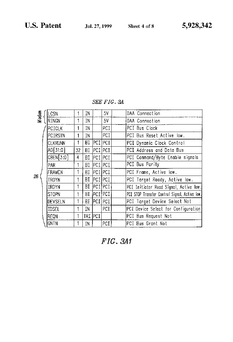
FIGS. 3A, 3A1 and 3B are a listing of the pin assignments
for the chip of FIG. 1.
FIG. 4 is a diagram illustrating the
location of different signals on the pins of the chip of FIG.
1.
FIGS. 5,6 & 7-9 are timing diagrams for certain sound
interfaces for a sound processor according to the present
invention.
DESCRIPTION OF THE PREFERRED EMBODIMENT
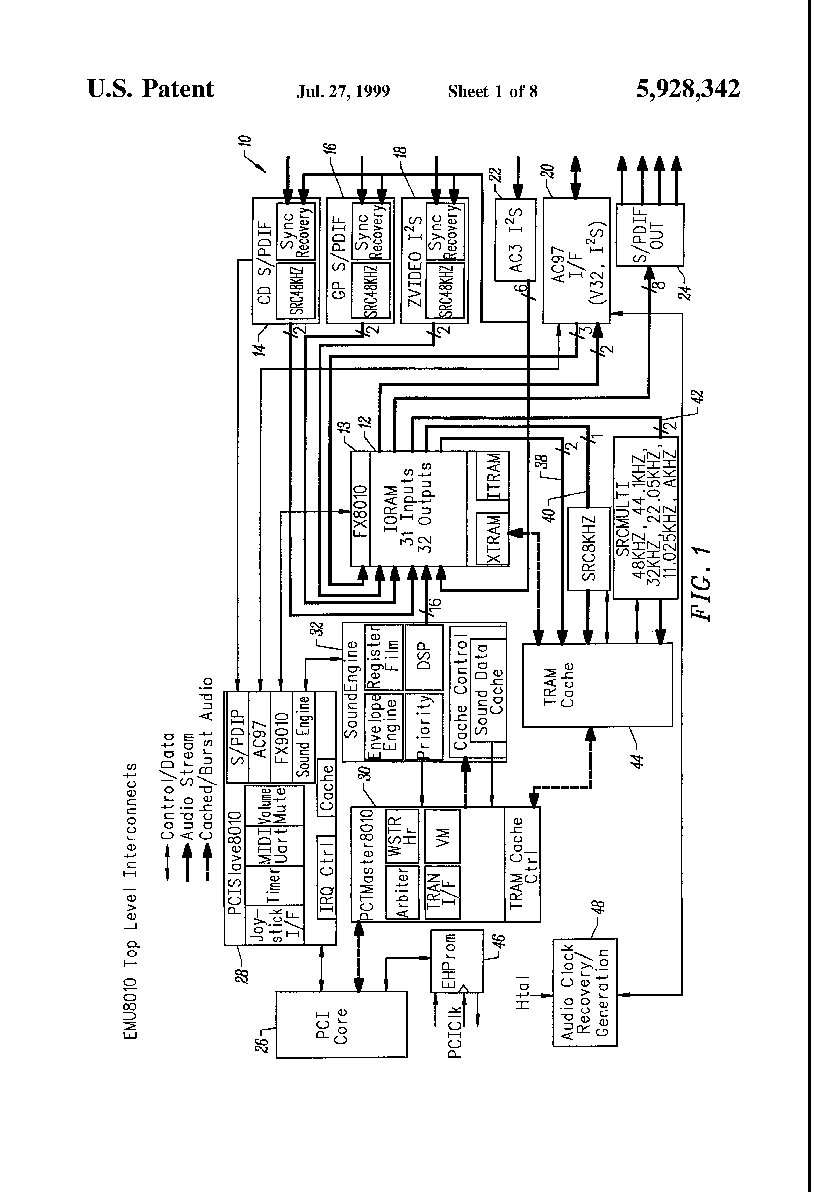
FIG. 1 is a block diagram of a sound
processor chip 10 according to the present invention. At
the center of the chip is a multi-port RAM memory 12,
which is used by a special purpose digital signal
processor optimized for enhancing audio, called the
effects engine 13. A number of buffer interfaces for
digital audio sample sources connect directly to ports of
memory 12. These interfaces include a CD-ROM SPDIF
interface 14, a general purpose SPDIF interface 16, a
ZVIDEO Audio I2 S interface 18 and a CODEC or ADC/DAC
interface 20. Optionally, an interface 22 for a AC-3
audio decompression and decoding chip is included.
Finally, six or eight channels of SPDIF output to
interface 24 are provided to four output pins.
Memory 12 can also receive sound samples from a host
memory. The interface with the host memory is over a PCI
bus through a PCI interface core 26. PCI slave circuitry
28 and master circuitry 30 connect to interface 26. Sound
samples can come in through PCI bus master 30 to a sound
engine 32 for processing, and from there can be stored in
memory 12.
In addition, a resampling path is provided through three
resampling streams 38, 40, and 42 to a tank RAM cache
(TRAM) 44.
Also provided is an EEPROM interface 46 for providing
default configuration register and other register values
from an external EEPROM for the PCI register values. In
addition, an audio clock recovery circuit 48 is provided.
FIG. 2 illustrates a typical sound board on
which an integrated circuit according to the present
invention may be mounted. Sound processor chip 10 is
shown mounted on a circuit board 50. Shown is a CDROM
connector 52 which couples to interface 14 of chip 10.
Also shown is an AC97 CODEC 54 which would connect to
interface 20 of FIG. 1. An optional AC-3 audio
decompressor/decoder 56 is shown for connecting to
interface 22. If an AC-97 CODEC is not used, discrete
components may be substituted, including a CODEC or
separate A/D and D/A converters and a mixer chip.
Also shown are various other connections to sound
processor chip 10, including a joystick connector 60, a
phone line connection for a modem 62, a line in connector
64, a microphone connector 66, and a speaker output 68.
In addition, a connection to a PCI bus 70 is shown. Bus
70 connects to the host microprocessor 72 and to main
memory 74. AUDIO I/O OVERVIEW
Audio I/O is accomplished by mapping I/O channel buffers
into the processor's general purpose register (GPR)
address space in memory 12. On each sample period,
signals from the input channels appear in the input GPRs,
and the contents of the output GPRs are written to output
channels. The GPR-mapping allows I/O channel buffers to
be used just like a GPR operand in any instruction of the
effect engine, with no restriction on reading or writing.
In general, audio I/O is multi-buffered, so that all
samples arrive and depart from the effects engine 13
synchronously. This means that input and output signals
for any I/O channel can be read or written at any time
during the sample period (i.e., from any instruction
step) and the signals are guaranteed to
"belong" to the same sample period.
Another feature of the I/O architecture is that the same
logical input and output channels share a common GPR
location. This means that when a signal flows in on a
particular channel, it will also flow out on that channel
if not altered by any instructions. Thus there is no
instruction overhead associated with simply moving
signals through the effects engine; if not otherwise
programmed, the effects engine acts as a digital
"wire" for the multi-channel audio stream
flowing through it. In fact, this is its default reset
behavior.
The overall structure of audio signal flow is shown in FIG.
1. The
effects engine 13 and memory 12 can be seen at the center
of this signal flow; it collects 16 audio channels from
the SoundEngine 32 as well as five additional streams
from external audio interfaces. The corresponding 21
output channels can be routed back to external interfaces
as well as to host memory, via the PCI bus.
A number of audio paths are running synchronously at a
(nominal) 48 KHz sample rate clock derived from the AC97
CODEC. This includes the sound engine 32, effects engine
13, AC97 CODEC interface 20 and S/PDIF outputs 24.
However, the interfaces also includes hardware to perform
sample-rate conversion to or from the local 48 KHz rate
on several other audio paths. These other paths can
interface with memory 12 through buffers in the
interface. These interfaces include CD-ROM interface 14,
general purpose SPDIF interface 16, and ZVIDEO interface
18.
All audio sources are 16 bits wide, and are
left-justified into the MSB position of the memory 12
GPRs; the least significant bits will be zero-filled.
Similarly, outputs are also 16 to 20 bits wide from the
same portion of the 32 bit wide GPR words. Output GPRs
are simply truncated before being passed out of the
memory 12; if desired, dithering can be performed in
microcode before the truncation occurs in hardware. A
special GPR-mapped dither noise source is provided for
this. Inputs
Sound Engine. The sound engine 32 is a 64-channel version
of the prior EMU8000 wavetable synthesis engine. One
difference is that any four of 16 output channels can be
selected as the destinations for each synthesizer voice,
with (smoothed) variable scaling on each of the four
ends. The 16 synthesizer output channels become 16 input
channels to the sound effects engine 13.
AC97. The AC97 interface supplies two (optionally three)
audio input channels at 48 KHz. In fact, the system clock
is usually derived from a clock shared by an AC97 CODEC;
thus the AC97 is the sample rate master for the entire
system.
In AC97 parlance, the three channels are known as the
optional microphone (mono) and ADC (stereo) channels. The
48 KHz microphone channel comes into memory 12 on the
same channel that is sent out to the 48 KHz to 8 KHz
sample-rate converter in feedback path 42 to the PCI
interface, so that no instructions are required to route
this signal.
Microphone Recording. The AC97 CODEC optionally contains
a third ADC which is intended for use as a monophonic
microphone input. Data from this ADC channel is routed at
48 KHz into the effects engine on input channel 20. The
corresponding effects engine output channel 20 is routed
into a sample rate converter which will convert the 48
KHz monophonic channel into an 8 KHz monophonic data
stream. If the microphone buffer size register (MBS) is
programmed to a non-zero value, this data stream is
transferred to a host memory beginning at the microphone
buffer base address (MBA). Audio data is accumulated in a
FIFO, then transferred to the host memory buffer in a
burst. When half the programmed buffer size is reached,
an interrupt will occur if the MBIE interrupt enable bit
in the interrupt enable (IE) register is set. A second
interrupt will occur when the end of buffer is reached,
at which time additional data will subsequently be
transferred at the start of the buffer. Transfer of data
will continue until the MBS is set to zero.
AC97 ADC Audio Input Recording. The AC97 CODEC contains a
stereo ADC producing a stereo digital audio stream at 48
KHz which is routed to the effects engine on two channels
for the left and right streams respectively. The
corresponding effects engine output feeds a stereo sample
rate converter, whose output can be written to a buffer
in host memory. The output rate of the sample rate
converter is determined by the ADC sample rate/stereo
control register (ADCSR). This register also controls
which channels will be written to host memory. A transfer
to host memory will occur as long as at least one channel
is enabled for write in the ADCSR register, and the ADC
buffer size register (ADCBS) is non-zero. If both
channels are enabled for writing to the host, the
transfer will always occur as pairs of interleaved left
and right 16 bit audio data words, with the left word at
the lower address. The transfer is enable, beginning at
the ADC buffer base address (ADCBA) by writing a non-zero
buffer size into the ADCBS register. Audio data is
accumulated in a FIFO, then transferred to the host
memory buffer in a burst. When half the programmed buffer
size is reached, an interrupt will occur if the ADCBIE
interrupt enable bit in the interrupt enable (IE)
register is set. A second interrupt will occur when the
end of buffer is reached, at which time additional data
will subsequently be transferred at the start of the
buffer. Transfer of data will continue until the ADCBS is
set to zero.
(CD-ROM) S/PDIF. The CD-ROM S/PDIF input on interface 14
is a sample rate converted, typically from 44.1 KHz to 48
KHz, and routed to two input channels. This is intended
to be the digital audio output from a CD-ROM drive
playing audio tracks, although the input can accept
S/PDIF data from any source.
GP S/PDIF. The GP S/PDIF input on interface 16 is sample
rate converted to 48 KHz, and routed to two input
channels. This general purpose accepts digital audio
output from any device producing S/PDIF format data.
ZVIDEO I2 S. The ZVIDEO I2 S input on interface 18 is
sample rate converted, typically from 22, 44, or external
48 KHz to the local 48 KHz rate, and routed to two input
channels. This is intended to be the digital audio output
from a ZVIDEO PCMCIA (PC-CARD) device, although the input
can accept I2 S data from any source.
AC-3 I2 S. The AC-3 I2 S input on interface 22 is
asynchronously sample rate converted, typically from 22,
44, or external 48 KHz to the local 48 KHz rate, and
routed to six input channels. This conversion shares the
same sample rate converter used by CD SPDIF interface 14,
GP SPDIF interface 16 and Z video interface 18.
The AC-3 interface will be enabled by setting a bit in
the Hardware Control Register. An additional bit will
control whether two channel or six channel data is
accepted. When disabled, the AC-3 data will be ignored by
the chip. When enabled in two channel mode, the AC-3
interface will take over the Z video interface, and
simply route the AC-3 stereo audio to that interface. Any
data appearing at the Z video inputs will be ignored.
When enabled in six channel mode, the AC-3 interface will
take over the Z video, the CD audio, and the GP SPDIF
interfaces. Channels 0 and 1 will be routed to the Z
video interface, channels 2 and 3 to the CD audio, and
channels 4 and 5 to GP SPDIF input. Data applied to the Z
video inputs will be ignored; data applied to the CD
audio and GP SPDIF inputs will be correctly reflected in
the associated channel status registers and associated
inputs, but the audio portion of these interfaces will
instead present the AC-3 data. Only 16 bits of data will
be presented. This is intended to be the digital audio
output from any external AC-3 audio decoder, although the
input can accept from two to six channel I2 S data from
any source. Outputs
AC97. The memory 12 supplies two channels back to the
same AC97 interface that is the source of the three input
channels and is synchronous with the master sample clock.
These two channels, running at 48 KHz, are considered the
"main" stereo outputs derived from the various
input sources via an output mixing and assignment
architecture implemented in microcode.
S/PDIF Output Channels. Six output channels are routed to
four auxiliary stereo S/PDIF output channels through
interface 24. These auxiliary channels run at 48 KHz
only, and may be considered to comprise a multi-track
"pro audio" interface to multi-track mixers or
surround-sound playback systems. This enables a class of
8-track professional audio applications.
Effects Engine Output Recording. Any or all of the
effects outputs can be written at their native 48 KHz
sample rate to a buffer in host memory. The effects
engine write channel (FXWC) register controls which
channels will be written to host memory. A transfer to
host memory will occur as long as at least one channel is
enabled for write in the FXWC register, and the effects
engine buffer size register (FXBS) is non-zero. If more
than one channel is enabled for writing to the host, the
transfer will comprise interleaved groups of 16 bit audio
data words, with the lowest channel at the lowest
address. If the number of channels to be transferred is
two, four, or eight, then the transfer will always result
in the same number of samples for each channel; if any
other number of channels is selected this is not
guaranteed to be true, and the stream should be
appropriately truncated by computing its size. The
transfer is enabled, beginning at the effects engine
buffer base address (FXBA) by writing a non-zero buffer
size into the FXBS register. Audio data is accumulated in
a FIFO, then transferred to the host memory buffer in a
burst. When half the programmed buffer size is reached,
an interrupt will occur if the FXBIE interrupt enable bit
in the interrupt enable (IE) register is set. A second
interrupt will occur when the end of buffer is reached,
at which time additional data will subsequently be
transferred at the start of the buffer. Transfer of data
will continue until the FXBS is set to zero. All
transfers of data to the host memory are 16 bit wide
audio samples. However, the effects engine can process
audio data up to 32 bits wide, and many of the input
audio sources can supply 20 bit audio data. By
programming the effects engine to split a wider audio
word into two outputs representing the most significant
and least significant parts of a 32 bit audio sample, the
facilities described above can be used to transfer 32 bit
audio data into host memory when required, using two
output channels for each 32 bit audio data stream.
Multi-track Resampling
Using the Effects Engine Output Recording, any or all of
the 32 effects outputs can be sent to host memory. This
mode of operation can be used to implement a multi-track
digital audio recorder when combined with the S/PDIF
output channels. The S/PDIF output channels represent the
audio output of the recorder, while the effects outputs
being transferred to host memory represent the input
being recorded into memory, and from there onto the
computer's hard disk for later playback.
Multi-Stream Recording. In addition to the effects engine
output, two other streams can be sent back over the PCI
bus to independent buffers in host memory. These streams
consist of:
A monophonic sample stream sample rate converted from the
local 48 KHz rate to 8 KHz (the AC97
"microphone" channel). The reduced data rate
will ease host data processing when the wide bandwidth is
not required, for example for telephony or speech
recognition applications.
A stereo sample stream converted to any of the following
rates: 48 KHz, 44.1 KHz, 32 KHz, 24 KHz, 22.05 KHz, 16
KHz, 11.025 KHz, or 8 KHZ.
Output Mixing. With a total of 21 channels flowing
through memory 12 from a variety of sources, there are
many possible approaches to an output mixing and channel
routing architecture. The best choice will depend upon
the specific applications for which the invention is
used. The default output mixer and channel router is
implemented in hardware, and simply passes each input
channel to each output channel. Any other strategy
requires a mixer implemented in the effects engine by
means of appropriate microcode. External Interface Timing
Clocks. The PCI interface logic operates on the PCI clock
and is synchronous with the PCI bus. The sound engine,
effects engine, and other portions of the audio
processing subsystem on the chip operate on a
1024×sample rate clock which is derived from and phase
locked to the CLK512 input from the AC97 chip, which is
the same 512×sample at a 48 KHz sample rate or 24.576
MHz (40.7 ns period) CLK512. Internally, the audio clock
is used for any functions requiring precise timing,
because the PCI clock frequency is not known. There are
asynchronous interfaces between the PCI bus logic and the
audio processing subsystem, which are accommodated by the
internal design.
PCI Interface. The PCI interface logic is designed to
meet all PCI specification 2.1 timing constraints. The
maximum PCI clock frequency is
33 MHz. The INTAN signal is asynchronous in nature and
does not have any timing constraints.
Joystick Interface Timing. The joystick pushbutton inputs
are polled when read by the host. No setup or hold time
is guaranteed. The joystick comparator pins are analog in
nature, and are designed to be compatible with existing
analog joystick circuits. No timing specifications beyond
this functionality are implied.
MIDI Interface Timing. The MIDI interface timing complies
with the MIDI 1.0 specification. The actual baud rate is
based on the nearest convenient integer divisor of the
24.576 MHz clock rate, in this case 784, giving 31.35
kbaud.
CD-ROM SPDIF Input Timing. The CD-ROM SPDIF input is
designed to accept an IEC-958 compliant signal at a
frequency of 32 KHz to 48 KHz +1/-10%.
General Purpose SPDIF Input Timing. The general purpose
SPDIF input is designed to accept an IEC-958 compliant
signal at a frequency of 32 KHz to 48 KHz +/-10%.
Volume and Mute Input Timing. The volume and mute control
inputs to the memory 12 are designed to be directly
connected to SPST pushbuttons to ground. These inputs
will accept noisy or bouncy signals whose bounce duration
is less than 50 msec. The maximum delay from switch
closure to interrupt is 10 msec.
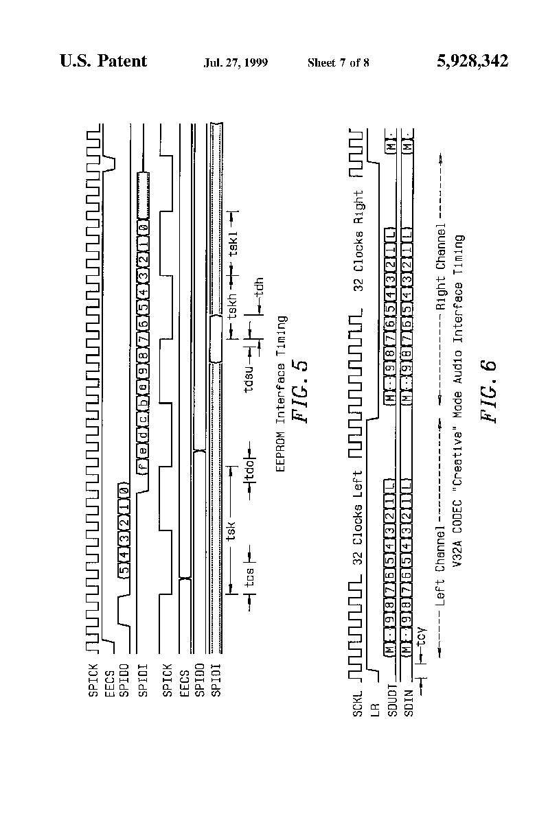
Generic 12S CODEC Interface Timing. The timing diagram of
FIG. 6 illustrates the serial audio data
interface when in "Generic 12S" mode.
MCLK runs at four times SCLK, with coincident rising
edges. MCLK runs at 256 times the 48 KHz sample rate,
SCLK at 64 times the sample rate, LR at the sample rate.
LR and SDOUT transition coincident with SCLK falling
edges. SDIN is sampled on SCLK rising edges. The MSB of
SDOUT and SDIN occurs one bit cell after the LR
transition. A total of 20 bits are supplied on SDOUT,
with the remaining 12 locations stuffed with zeros. A
total of 20 bits are recognized on SDIN, with the
remaining 12 locations ignored.
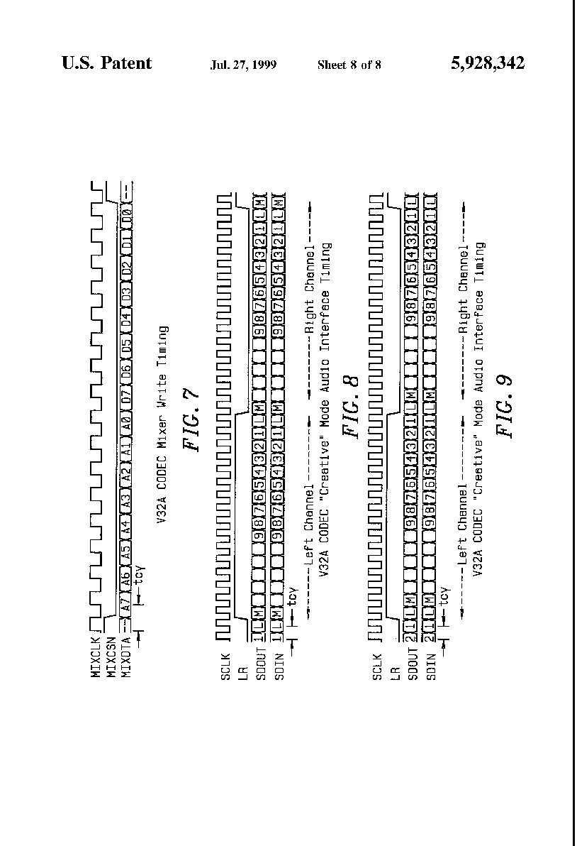
V32A Interface Timing. The chip 10, when configured for
operation with the V32A, meets the specification of the
Creative V32A CODEC, version 0.10. The timing diagram of FIG. 7 illustrates the mixer interface
timing during write.
Tcy is nominally 81.38 nsec, with nominally 50% duty
cycle. MIXCLK (from pin AC97RSTN) falling edge is
coincident with MIXCSN and MIXDTA transitions.
The timing diagram of FIG. 8 illustrates the serial audio data
interface to the V32A in "Creative" mode.
MCLK runs at eight times SCLK, with coincident rising
edges. MCLK runs at 256 times the 48 KHz sample rate.
SCLK at 32 times the sample rate, LR at the sample rate.
LR and SDOUt transition coincident with SCLK falling
edges. SDIN is sampled on SCLK rising edges.
The timing diagram of FIG. 9 illustrates the serial audio data
interface to the V32A in "12S" mode.
Operation in this mode is identical with
"Creative" mode except that both SDOUT and SDIN
have been shifted one bit later in time to correspond
with the 12S format.
AC97 Interface Timing. The AC97 interface is designed to
meet the specifications of the AC97 specification,
revision 1.00.
EEPROM Interface. The load time of the EEPROM is less
than 10 msec, which occurs within
"initialization" time on the PCI spec, and
therefore does not have to meet the eight or 16 clock
rules. If configuration space is accessed prior to
completion of EEPROM load, excessive wait states will
result, but this is within PCI 2.1 specifications.
The chip 10 contains an interface 46 to a 93C46 type
EEPROM, which is used on reset to configure the PCI
interface. On the trailing edge of PCIRSTN, the EEPROM is
read via the EEPROM serial interface, and the contents
are used to establish the programmable PCI configuration
registers. FIG. 5 shows the interface timing
for the EEPROM. Note that if the SPIDI pin is resistively
tied to either ground or the supply, the default values
of the PCI configuration registers are used, thus
enabling a "zero glue" usage of chip 10. Tying
EESDI to ground will enable the joystick function. Tying
it to the power supply will cause the joystick function
to be disabled.
The format for the "FuncEnbs" bytes is a `1` in
the bit position corresponding to the PCI function number
to enable the function. Function 0 is always enabled. The
values in bits 0, 3, 4, 5, 6, and 7 are don't care and
conventionally zero, and the value in bit 1 indicates
that the joystick is enabled (1) or disable (0), while
the value in bit 2 indicates that the modem is enabled
(1) or disabled (0). NOTES:
1. The times provide for the standard 93C46 memory, and
result in a complete read time for all 1024 bits of
memory in less than 10 msec.
2. tSK is derived from the audio clock and is 50% duty
cycle at 384 Khz.
3. After the EEPROM has been read, EECS will remain low
until another PCI reset trailing edge occurs. Subsequent
to this, SPICK, SPIDI and SPIDO could be used by other
functions needing a serial interface such as the SPI
interface.
Pin Descriptions
- JOYPB[3:0]--These four input pins with pullups connect
to the joystick push-buttons and receive their state.
- JOYCMP[3:0]--These four Schmidt trigger input pins
connect to the joystick pullup and capacitor network.
When the joystick is triggered, these pins are output
enabled and discharge the capacitor. The period of time
until they return to a valid logic high is timed, and the
count is used as the joystick axis value.
- INMIDI--This input pin receives data intended for the
sound processor chip's MIDI UART. The polarity is such
that a start bit is a logic low level.
- OUTMIDI--This input pin provides data from the MIDI
UART. The polarity is such that a start bit is a logic
low level. Note that to comply with the MIDI 1.0
specification, a buffering transistor must be used.
- CDROMI--This input receives the SPDIF format digital
audio data from the CD-ROM or other SPDIF digital audio
source operating at a sample rate between 28 KHz and 53
KHz.
- GPSPDIF--This input receives the SPDIF format digital
audio data from a general purpose digital audio source
operating at a sample rate between 28 KHz and 53 KHz.
- SPDIFO[3:0]--These four output pins provide four stereo
channels of SPDIF format digital audio data from the
sound processor chip at a fixed 48 KHz rate.
- VOLINCN--This input with pullup is connected to the
volume increment push-button.
- VOLDECN--This input with pullup is connected to the
volume decrement push-button.
- ZVSD--This input is the I2 S format Zoomed Video serial
data.
- ZVSCK--This input is the I2 S format Zoomed Video
serial bit clock.
- ZVLRCK--This input is the I2 format Zoomed Video serial
left/right word clock.
- AC97BCK--This input receives the 12.288 MHz rate bit
clock from the AC97 CODEC. When in other CODEC modes,
this pin is unused.
- AC97SDI--This input receives serial data from the AC97
or other CODEC.
- AC97SYNC--This output provides the sync signal to the
AC97 CODEC. When in other modes, this pin supplies the
frame sync (Left/Right) signal to the CODEC.
- AC97SDO--This output provides the serial data to the
AC97 or other CODEC.
- AC97RSTN--This output provides the reset signal to the
AC97 CODEC. When in other modes, this pin supplies a
12.288 MHz clock, which will also serve as the MIXCLK for
the V32A interface.
- MIXCSN--This output provides the Chip Select to the
V32A CODEC.
- MIXCLK--Bit clock to the V32A CODEC.
- MIXDTA--This output provides the Mixer Serial Data to
the V32A CODEC.
- EECS--This output provides the chip select signal to
the external EEPROM.
- EECLK--This output provides the serial clock signal to
the EEPROM.
- EESDO--This output provides the serial data signal to
the external EEPROM during power on reset configuration.
- EESDI--This input receives the serial data signal from
the external EEPROM. If no EEPROM is used, this pin can
be resistively pulled to power or ground. When the EEPROM
read is attempted after the trailing edge of PCI reset,
this passive state will respectively disable or enable
the analog joystick interface function respectively.
- AC3FS--This input is the I2 S format left/right frame
sync clock from the AC3 decoder for the decoded data
streams.
- AC3DBCK--This output is the I2 S format bit clock to
the AC3 decoder for the decoded audio data.
- AC3DSD0--This input receives the left and right front
channels in I2 S format from the AC3 decoder.
- AC3DSD1--This input receives the left and right
surround channels in I2 S format from the AC3 decoder.
- AC3DSD2--This input receives the center and subwoofer
channels in I2 S format from the AC3 decoder.
- PULSEN--This output supplies the host modem subscriber
line interface "pulse" information.
- HOOKN--This output supplies the host model subscriber
line interface "hook" information.
- HANDN--This output supplies the host modem subscriber
line interface "hand" information.
- LCSN--This input receives the host modem subscriber
line interface "ics" information.
- RINGN--This input pin receives the host modem
subscriber line interface "ring" information.
- PCICLK--This input is connected to the PCI
"CLK" clock signal. The sound processor chip is
specified to operate with PCI clock frequencies to 33
MHz.
- PCIRSTN--This active ow input is connected to the PCI
"RST#" reset signal. This signal activates
manufacturing test modes in the sound processor chip when
combined with other signals.
- CLKRUNN--This bi-directional pin as an input warns the
PCICLK will be stopped in four PCI clocks. As an open
drain output the sound processor chip can signal that it
needs more time before clock can be stopped.
- AD[31:0]--These bi-directional pins are connected to
the PCI "AD[31::0]" multiplexed address/data
bus.
- CBE[3:0]N--These active low bi-directional pins are
connected to the PCI C/BE[3::0]# command/byte enable bus.
- PAR--This bi-directional pin is connected to the PCI
"PAR" parity pin.
- FRAMEN--This active low bi-directional pin is connected
to the PCI "FRAME#" cycle frame pin.
- TRDYN--This active low bi-directional pin is connected
to the PCI "TRDY#" target ready pin.
- IRDYN--This active low bi-directional pin is connected
to the PCI "IRDY#" initiator ready pin.
- STOPN--This active low bi-directional pin is connected
to the PCI "STOP#" stop pin.
- DEVSELN--This active low bi-directional pin is
connected to the PCI "DEVSEL#" device selected
pin.
- IDSEL--This input pin is connected to the PCI
"IDSEL" initialization device select pin.
- REON--This active low tri-state output pin is connected
to the PCI "REQ#" bus request pin.
- GNTN--This active low input pin is connected to the PCI
"GNT#" bus grant pin.
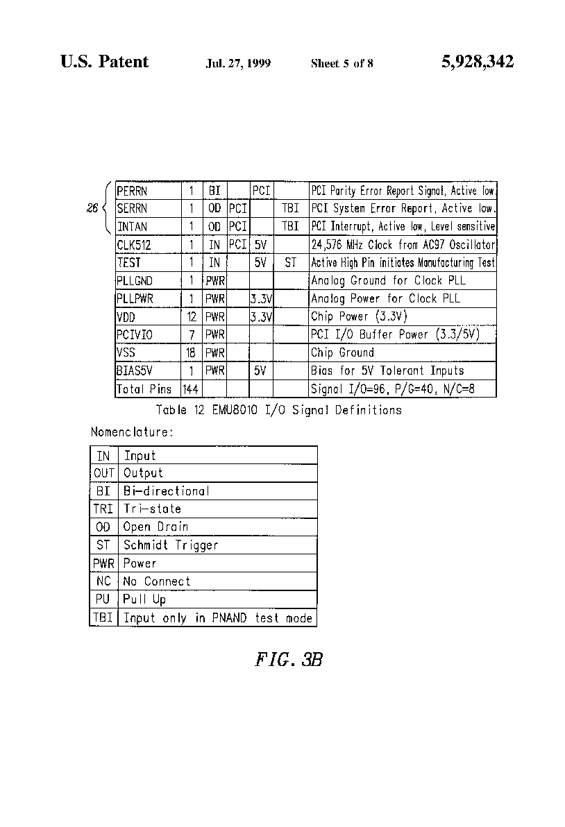
- PERRN--This active low bi-directional pin is connected
to the PCI "PERR#" parity error pin.
- SERRN--This active low open drain output pin is
connected to the PCI "SERR#" system error pin.
- INTAN--This active low open drain output pin is
connected to the PCI "INTA#" interrupt A pin.
- CLK512--This input pin connects to the AC97 CODEC
Master oscillator, and receives a 24.576 MHz (512×48
KHz) clock, which will be used by the on-chip PLL to
produce the internal audio clocks.
- TEST--This input is asserted high to implement
manufacturing test modes in the sound processor chip.
This pad does not include a pull-down resistor so that
IDDQ testing may be performed.
- PLLPWR--This input pin supplies +3.3 V power to the
internal clock PLL analog circuit block.
- REFCAP--This input pin supplies decoupling for the
internal clock PLL analog circuit block.
- VDD--These power input pins supply +3.3 V power to the
pads and core of the sound processor chip.
- VIO--These power pins supply the PCI reflected wave
buffers only. They can be either 3.3 or 5 V depending on
the PCI signaling environment.
- VSS--These power input pins supply ground to the pads
and core of the sound processor chip.
- BIAS5V--This power input pin supplies the bias voltage
for the 5 V tolerant input pads not associated with the
PCI bus.
As will be understood by those of skill in the art, the
present invention may be embodied in other specific forms
without departing from the spirit or essential
characteristics thereof. Accordingly, the foregoing
description is intended to be illustrative, but not
limiting, of the scope of the invention which is set
forth in the following claims.